|
||||||
Мини DDS VFO.
This is NOT meant as a detailed building instruction
for a DDS VFO. It is only a few fragments from my experimental work in the shack. This is "as is"
information. It may contain errors. However, my own prototype works very well.
If you find this VFO interesting and want more information, or if you run into problems, such as
missing information, errors etc, please contact me via email: sm6lkm.jbeab@swipnet.se
|
|
WHAT'S THIS?
This is a 0 - 6 MHz DDS VFO controlled by a PIC16C84.
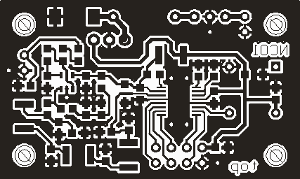
The VFO is separated into two modules, the DDS module and the controller module. The PCB layout (double sided) for
the DDS module is included as two Postscript files (scale 1:1). The .PS files can be copied to a Postscript
capable printer such as HP LaserJet 4MP. Please note that the layout is mirrored to get the toner side of the film
toward the PCB surface.
 Check the text on the layout to make sure that you don't
make a mirrored PCB!
There is no PCB layout for the controller. The controller is so simple, it can be built on a piece of
Veroboard.
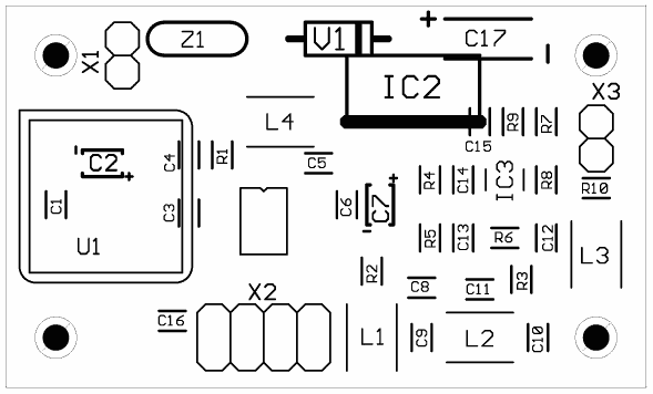
Most of the components are surface mounted on the top side of the DDS module
board. The through-hole components are
mounted on the bottom side (but soldered on the top side). There are a few via holes for ground connection between
top and bottom. Solder thin wires through these holes before you start to solder the
components. It doesn't hurt to drill a few more via holes in addition to those
shown on the layout. I made extra ground vias between L2
and L3 (at the board edge close to C10), close to the ground pin of oscillator U1 and close to the grounded end
of C17.
Bend the pins of the voltage regulator, IC2, so that the TO-220 case is laying on the ground
plane. The top of the cooling tab can be soldered to the ground plane for
mechanical stability.
A "canned" oscillator is not the best choice for high stability but it provides an easy way to get
going...

CONTROLLER PROGRAM
The PIC program is a prototype. Some of the code has been borrowed from another DDS control program (for AD9850)
written by Curtis W. Preuss, WB2V. The current version has the following functions:
- Rotary encoder input for tuning
- Dial lock switch
- Step size switch (1, 10, 100, 1 kHz, 10 kHz)
- LCD interface, shows frequency, in Hz) and step size
- f/4 display possible (for I/Q front ends using LO divider)
The smallest step size is 1 Hz (although the AD9832 is able to tune in 5.8 mHz (millihertz!) steps).
The PIC interfaces to a standard 1x16 LCD which is run in 4-bit mode. Almost any LCD with Hitachi HD44780 controller will work.
My prototype uses a PIC16C84 (discontinued?) but the program will run equally well on a PIC16F84 with minor modifications
(there are some differencies in the CPU configuration word). The 'F84 also contains more RAM which can be useful when
adding "bells and whistles" to the program.
Since the PIC controller is not onboard the DDS module, there is no reason why you couldn't use, for example, your PC to
control it through the printer port. Only three lines are needed to control the AD9832 (data, clock and strobe). Have
a look at the AD9832 data sheet for detailed information. (Available in PDF format from
http://www.analog.com). AD9850 and AD9851 data sheets are also worth reading for
general DDS information.

CONTROLLER HARDWARE
PIC16C84
|----\/---|
LCD D6, DDS SCLK -----| RA2 RA1 |--- LCD D5
LCD D7, DDS SDATA ----| RA3 RA0 |--- LCD D4
F/4 select ----------| RA4 OSC1|--- XTAL a, 22pF to GND
4k7 pullup to +5V ----|MCLR OSC2|--- XTAL b, 22pF to GND
Ground ---------------| VSS VDD |--- +5V
Encoder phase A ------| RB0 RB7 |--- DDS FSYNC
Encoder phase B ------| RB1 RB6 |--- LCD E
Step switch to GND ---| RB2 RB5 |--- LCD R/W
Lock switch to GND ---| RB3 RB4 |--- LCD RS
|---------|
* D0 to D3 on the LCD module are not connected.
* RA2 and RA3 are connected to both LCD and DDS.
* F/4 pin (RA4):
0 - LCD shows actual output frequency
1 - LCD shows output frequency divided by 4
* The inputs for step pushbutton and lock switch
do not need pull-up resistors (they have internal
pull-up in the PIC).
* XTAL is 4 MHz.
* Decouple +5V to GND close to the PIC with 0.1 uF ceramic.
* The controller can be powered from the DDS module.
* If the encoder is running backwards, swap RA0 and RA1.
* X2 connector on DDS module as viewed from bottom side:
Osc. U1 here
PSEL1 FSYNC SDATA +5V
o o o o
o o o o
PSEL0 FSEL SCLK GND
------ board edge here ------
PSEL0, PSEL1 and FSEL should be connected to ground
when this controller is used.
DDS MODULE COMPONENTS
C1 0.1 uF ceramic, size 0805
C2 4.7 uF 6V tantalum, size EIA3216
C3 0.1 uF ceramic, size 0805
C4 0.01 uF ceramic, size 0805
C5 0.01 uF ceramic, size 0805
C6 0.1 uF ceramic, size 0805
C7 4.7 uF 6V tantalum, size EIA3216
C8 82 pF ceramic, size 0805
C9 180 pF ceramic, size 0805
C10 180 pF ceramic, size 0805
C11 82 pF ceramic, size 0805
C12 1 uF ceramic, size 0805
C13 1 uF ceramic, size 0805
C14 0.1 uF ceramic, size 0805
C15 1 uF ceramic, size 0805
C16 0.1 uF ceramic, size 0805
C17 4.7 uF 25V tantalum, size EIA6032
IC1 AD9832BRU (Analog Devices)
IC2 7805 (TO-220 size)
IC3 MAX4012 (Maxim)
L1 10 uH Coilcraft 1812CS
L2 12 uH Coilcraft 1812CS
L3 10 uH Coilcraft 1812CS
L4 10 uH Coilcraft 1812CS
R1 3.9 k size 0805
R2 300 ohms size 0805
R3 330 ohms size 0805
R4 11 k size 0805
R5 1.5 k size 0805
R6 3.3 k size 0805
R7 470 ohms size 0805
R8 150 ohms size 0805
R9 47 ohms size 0805
R10 10 k size 0805
U1 25 MHz (for example IQD IQXO-22)
V1 1N4007
X1 2x1 pin strip, 0.1" spacing
X2 2x4 pin strip, 0.1" spacing
X3 2x1 pin strip, 0.1" spacing
Z1 Murata DSS306-55FFZ103N100, 0.01 uF
![]() Здесь полный комплект
документации:
Здесь полный комплект
документации:
compplac.pdf Component placement in PDF format
schema.pdf Schematic diagram in PDF format
top.ps PCB top copper layer in Postscript format
bottom.ps PCB bottom copper layer in Postscript format
ad9832_3.asm PIC16C84 source code
p16c84.inc Needed for assembly of ad9832_3.asm
vfo5x10.hex PIC program for LCD with 5x10 font
vfo5x7.hex PIC program for LCD with 5x7 font (not tested)
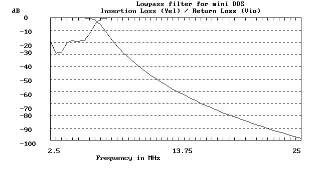
filtresp.pcx Computed frequency response of lowpass filter
73 de Johan Bodin, SM6LKM
J. Bodin (SM6LKM), sm6lkm.jbeab@swipnet.se